4 Layer Pcb Design Guide
Why do we use 4 layer pcb? The number of layers used for a pcb depends on the application, the operating frequencies, pin density, and the requirement for signal layers.
Pcb Layout 4 Layer PCB Circuits
Similarly for rf routing on the layer between the ground planes or

4 layer pcb design guide. This document is a guideline for designing a carrier board with high speed signals that is used with toradex computer modules. A pcb layer is made up of signal transmitting levels that are vertical to the board's plane. Type of pcb based on their flexibility sometimes, printed circuit boards are classified based on their flexibility, which defines what applications they can be used for.
A layer is the signal conducting levels that are vertical to the pcb plane. These layers are responsible for assembly or building a pcb. Designs of 2 layers pcb and 4 layers pcb.
Here, routing can be made on all the four layers which helps us to do more. Most often, one of these will be a. Needless to say, the surface is two times larger than a 1 layer pcb.
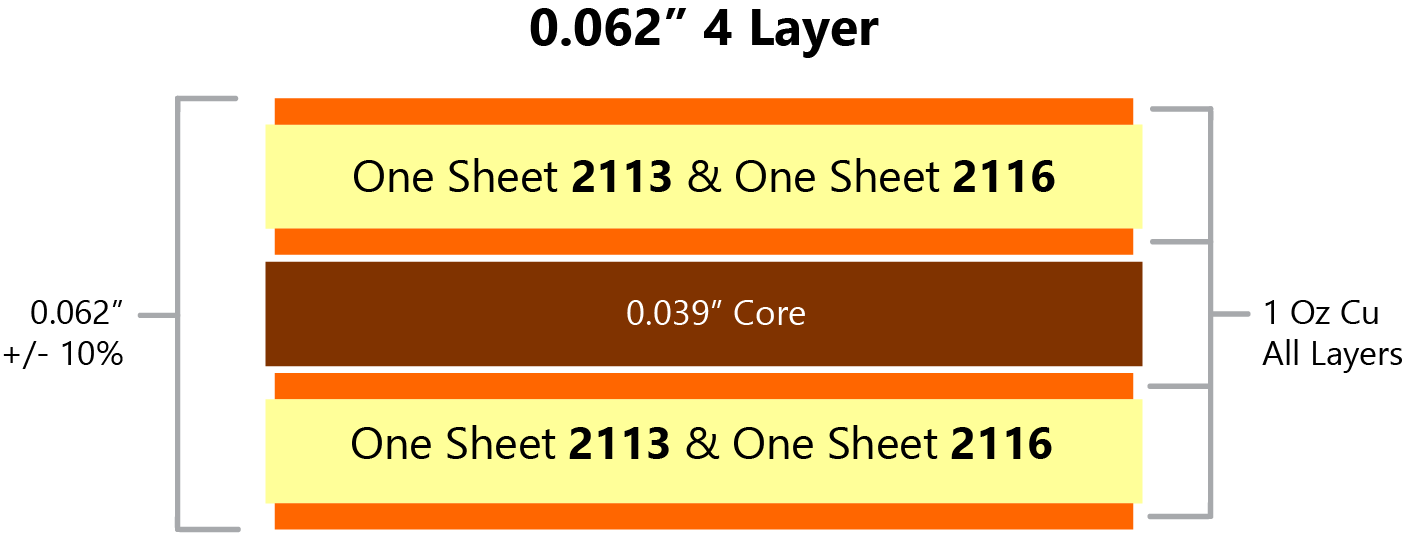
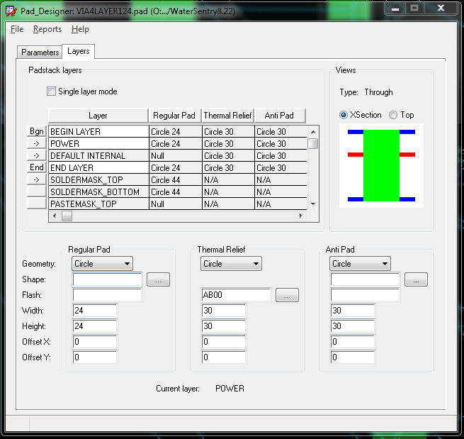
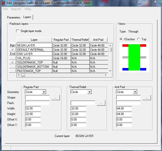
As shown in the figure above, a 4 layer stackup includes two internal layers. Ensure you have wide enough traces (100 mils is fine for 5 to 10 a), and don't daisy chain power lines. This means that your board will include blind vias.
For a 4 layer pcb, for instance, you'll find a top, inner 1, inner 2, and bottom layer. Pcb manufacturing porcess flow chart; Jinghongyi pcb (hk) co., limited [guangdong,china].
We call it inner layer 1 and inner layer 2. In this example, as copper thickness is stable, pcb maker will adjust thickness of prepreg and core to meet thickness need. In the case of a 4 layer pcb, there are actually 4 layers of conductive copper material.
For components that need direct connections to power, it's recommended to use common rails for each supply if a power plane is not used; And vias in 2 layers pcb are used to create electrical connections that can achieve the routing of the traces to get to the opposite. Hence, you'll find a 2 layer pcb having a top and bottom layer.
Although, it is possible to design a 3 layer board with a power plane, practically, a 4 layer pcb, shown in the figure below, is most likely the smallest stackup that will contain a power layer. There're 2 methods to be compatible with the adjustment mentioned above. Layout design guide toradex ag l altsagenstrasse 5 l 6048 horw l switzerland l +41 41 500 48 00 l www.toradex.com l info@toradex.com page | 2 issued by:
On one hand, the design of 2 layers pcb can offer more surface area for including a conductor pattern. Each zone or board region associates with a specific layer stack. Resin recession groove is used in board side design instead of.
Altium designer offers advanced pcb layer stack management
4 Layer Pcb Design In Orcad PCB Designs

Lpddr4 Pcb Layout Guidelines PCB Circuits
Ti Pcb Layout Guide PCB Circuits
6 Layer Pcb Design Guidelines Pcb Circuits
6 Layer Pcb Design Guidelines Pcb Circuits

China Cheapest Factory 4 Layer Pcb Fabrication HDI

4 Layer Pcb Design Rules Design Pcbs For Emi Part 2

2 Layer PCB 2 Layer Vs. 4 Layer Printed Circuit Boards
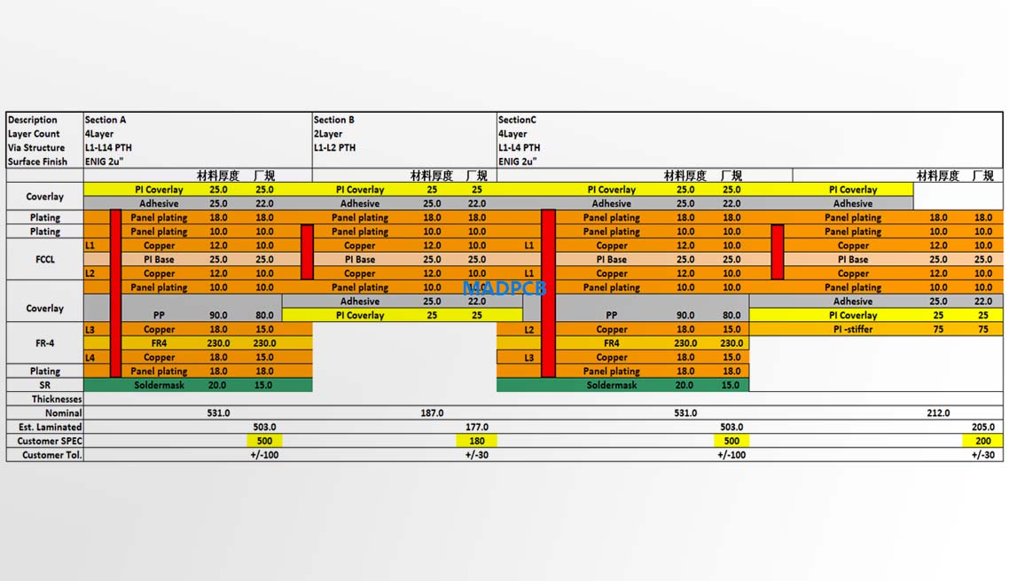
4Layer RigidFlex PCB with Blind Vias PCB Manufacturer

No Copper Fill for Inductor On All Layers (4 layer design
4 Layer Pcb Design Tutorial Orcad PCB Designs

4 Layer Pcb Layout Guide PCB Board
4 Layer Pcb Design In Orcad PCB Designs
DesignLeitlinien Eurocircuits


Pcb Layout 4 Layer PCB Circuits
4 Layers High Density PCB Layout With Immersion Gold Pads
4 Layer PCB Layout Using EasyEDA Step By Step Tutorial

BGA Design in 4 layer PCB Circuit Routing and Pin

Pcb Layout 4 Layer PCB Circuits